Analysis of Impedance, Input Impedance, and Output Impedance
Impedance is a collective term for resistance and reactance, and the biggest difference between resistance and reactance is that resistance current limiting (Ohm's law) consumes electrical energy at the same time. Reactance is limited to current and does not consume electrical energy (without doing work). Resistance has a limited current effect in both direct current and alternating current, while reactance only has a limited current effect in alternating current environments.
Input impedance refers to the equivalent impedance at the input end of a circuit. Add a voltage source U to the input terminal and measure the current I at the input terminal, then the input impedance Rin is U/I. You can imagine the input end as the two ends of a resistor, and the resistance value of this resistor is the input impedance.
Under the same input voltage, if the input impedance is very low, a large current needs to flow, which tests the current output ability of the previous stage; If the input impedance is high, only a small amount of current is required, which reduces a significant burden on the current output capability of the front stage. So in circuit design, try to increase the input impedance as much as possible.
The input impedance is no different from an ordinary reactance component, as it reflects the magnitude of the current blocking effect.
For voltage driven circuits, the larger the input impedance, the lighter the load on the voltage source, making it easier to drive without affecting the signal source; For current driven circuits, the smaller the input impedance, the lighter the load on the current source.
Therefore, we can think that if a voltage source is used to drive, the larger the input impedance, the better; If it is driven by a current source, the smaller the impedance, the better (note: only suitable for low-frequency circuits, in high-frequency circuits, impedance matching should also be considered.) Additionally, when obtaining maximum output power, impedance matching should also be considered.
Output Impedance
The output impedance includes the internal impedance of the equivalent voltage source (Thevenin equivalent circuit) or equivalent current source (Norton equivalent circuit) of the independent power network output port. Its value is equal to the input impedance seen from the output port when the independent power supply is set to zero.
Regardless of the signal source, amplifier, and power supply, there is an issue with output impedance. The output impedance is the internal resistance of a signal source. Originally, for an ideal voltage source (including power supply), the internal resistance should be 0, or the impedance of an ideal current source should be infinite. The output impedance needs the most special attention in circuit design.
In reality, voltage sources cannot achieve this, and an ideal voltage source is often connected in series with a resistor r to equivalent an actual voltage source. The resistor r in series with the ideal voltage source is the internal resistance of the signal source/amplifier output/power supply.
When this voltage source supplies power to the load, a current I will flow through the load and generate I on this resistor × The voltage drop of r. This will result in a decrease in the output voltage of the power supply, thereby limiting the maximum output power.
Similarly, an ideal current source should have an output impedance of infinity, but actual circuits are impossible.
Output impedance refers to the equivalent impedance of the circuit when the circuit load is viewed from the output port of the circuit in the opposite direction. In fact, it mainly refers to the impedance measured by the energy source at the output end, commonly known as internal resistance.
Impedance Thinking Analysis of Switching Circuits
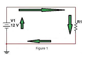
As shown in the following figure, V1 continues to deliver current to R1, and the current circuit in the figure is shown by the green arrow. What methods do we have if we want to control the current flow to R1?
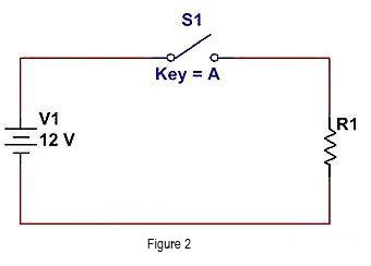
The most common method is to disconnect the connection between V1 and R1 and cut off the current circuit. As shown in the following figure.
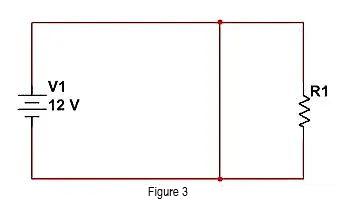
Alternatively, we can bypass R1 as shown in the following figure. Add a wire in front of R1 to direct the current towards the path with low impedance, and R1 will obtain negligible current.
The above two methods are very straightforward, either completely disconnecting the path from V1 to R1 or short circuiting R1, which solves the problem thoroughly. But in the world of engineering, we cannot do it so cleanly and neatly, often emphasizing a 'similar' approach. So, in the "short circuit model", we can only achieve "low impedance", while in the "open circuit model", we can only achieve "high impedance". If the energy is significantly "attenuated", we believe that it meets the standard.
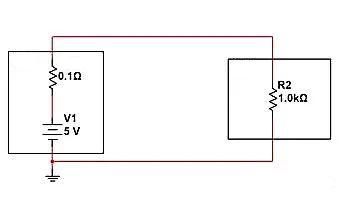
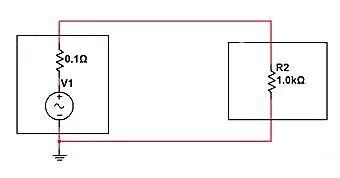
As shown in the figure below, the actual power load model is shown. Let's see how to achieve switching effect by adjusting impedance. In actual circuits, power sources have output capacity limitations and internal resistance, and the larger the output current, the lower the output voltage.
The following circuit has an internal resistance of 0.1 Ω and a load of 1K Ω. In the current situation, the voltage obtained at both ends of the load is composed of internal resistance and R2 partial voltage. We can calculate V=5V * (1K/(1K+0.1))=4.9999V, I=5V/1000.1 Ω=4.9mA.
If we use the "open circuit model" method to break the circuit, how should we adjust the impedance? It is to connect a resistor that is much greater than 1K in series between the power supply and the load, and perform series voltage division to reduce the voltage obtained on R2. As shown in the following figure, if a 1M resistor is connected in series with the load voltage divider. We can calculate the final voltage distribution between the two ends of the load:
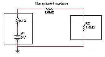
V=5V * (1K/(0.1+1000K+1K))=0.00499V, I=5V/1001000.1 Ω=0.0049mA. The amplitude has been weakened by nearly 1000 times, and in engineering thinking, R2 is almost "disconnected".
If we use the "short circuit model" method to disconnect R2, how should we adjust it? It is to connect a resistor that is much smaller than 0.1 Ω in parallel at the front end of the load and perform series voltage sharing with the internal resistor, resulting in a smaller voltage obtained on R2.
As shown in the following figure, if the filtering measure is equivalent to a parallel 0.005 Ω resistor and internal resistance voltage divider. We can calculate the final distributed voltage between the two ends of load R2:
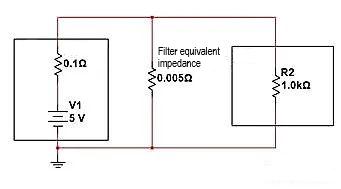
V=5V * (0.0049/(0.1+0.0049)=0.233V. The amplitude has been weakened by nearly 20 times, and in engineering thinking, R2 is also similar to being "disconnected".
The above is the theoretical model of semiconductor switch circuits, taking inverter circuits as an example:
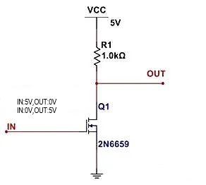
When the IN end is powered up, we will say that MOS transistor Q1 is conducting. At this point, the conduction state is equivalent to Q1 becoming a resistor with an impedance of tens of milliohms, and then dividing the voltage with R1 resistor. If the pull-up resistor R1 is too small and also tens of milliohms, even if IN is high and Q1 is conducting, the OUT terminal cannot output a low level.
When the IN end is powered down, we will say that the MOS transistor Q1 is cut off. At this point, the cutoff state is equivalent to Q1 becoming a resistor with an impedance of a few megaohms, and dividing the voltage with R1 resistor. If the pull-up resistor R1 is too large, which is also a few megaohms, even if IN is low and Q1 is cut off, the OUT terminal cannot output a high level.
So when deeply understanding switch circuits, it is necessary to analyze them with impedance thinking.
Impedance Thinking Analysis Filter Circuit
Here, analyze the filtering circuit using impedance thinking.
In practical engineering applications, a power output often contains AC components of different frequencies, both what we want and what we don't want. The impedance of inductance and capacitance will vary with frequency. It is precisely because of this characteristic that inductors and capacitors have become the leading actors in filtering circuits.
The following circuit is still used, assuming that the power supply contains a spectral component of
0-1GHz.
If we want to filter out high-frequency AC components for load R2, we will find that both series inductance and parallel capacitance can meet the requirements.
As shown in the following figure, if one 16uH inductor is connected in series between the power supply and load, how much will the 100MHz AC component decay? According to the impedance formula of inductance: ZL=2 π fL=2 * 3.14 * 100MHz * 16uH, ZL=10K can be obtained.
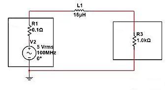
According to the series voltage divider formula, the voltage/input at both ends of R3=R3/(R3+ZL)=1K/11K=0.0909. So when the power supply amplitude is 5V, the amplitude at both ends of R3 is only 5V * 0.0909=0.45V.
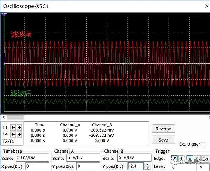
At 100MHz, use an oscilloscope to measure the waveform before and after filtering. The comparison shows that the 100MHz waveform has an effect, and the actual measurement is 0.449V, which is consistent with the analysis results.
Impedance thinking analysis of low-pass filters
By connecting an inductor in series between the power supply and the load, and connecting a capacitor in parallel at the front end of the load, a low-pass filter circuit is formed.
As follows, if C1=1uF and L1=22uH, what is the attenuation degree of the filtering circuit to the
100MHZ AC component?
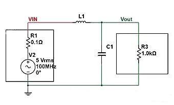
At this point, the circuit is connected in parallel with the impedance Zc of capacitor (C1) and R3, and then divided with the impedance ZL of inductor (L1). So we can list the impedance equation (which is a simple series voltage divider formula).
Attenuation amplitude=Vout/Vin=(Zc//R3)/(ZL+(Zc/R3)
Among them, Zc=1/2 π fC and ZL=2 π fL. Given R3=1K Ω, it can be concluded that Zc=0.0015 Ω, Zc/R=0.00149 Ω.
ZL=13816 Ω, the attenuation amplitude can be obtained as 0.00149/(13816.00149)=0.000000178.
It can be seen that the 100MHz AC component can hardly pass through the low-pass filtering circuit of 22uH and 1uF. At the same time, we also see that the load R3 can affect the filtering effect of the filter. So sometimes we find that the same filter circuit works well on this circuit, but poorly on other circuits.
tags :
categories
recent posts


scan to wechat:everexceed